-

- June 12, 2023
- PCB knowledge
- (0)
- 08 mins
PWB – Unraveling the Significance of PWB in the Electronics Industry
PWB, or Printed Wiring Board, is a term that has gained prominence in the electronics industry. This crucial component forms the foundation of numerous electronic devices. But what exactly is a PWB?

A PWB is a board that serves as the ‘skeleton’ for electronic devices. It offers a platform where different device components are connected, ensuring the smooth flow of electric current from one point to another.
Interestingly, a PWB is not just a simple board. It is a meticulously designed and precisely manufactured component that withstands varying levels of electric current. It is carefully constructed to meet the requirements of the specific device in which it is being used.
But why is it called a ‘Printed Wiring Board’?
The term “printed” stems from the manufacturing process. The wiring, or circuit design, is ‘printed’ or etched onto the board, forming a complex network of conductive pathways. These pathways are responsible for transporting electric signals across the device, enabling it to perform its intended function.
PWB and PCB are two terms that often confuse, even among those familiar with electronics. While they share similarities, they are not synonymous.
PWB stands for Printed Wiring Board, while PCB stands for Printed Circuit Board. It’s important to note that every PCB is a PWB, but not every PWB is a PCB. This statement may initially seem paradoxical, but let’s break it down.
A PWB refers to a board that contains only the wiring layout. It’s the foundational platform on which all the components will eventually be placed. At this stage, it’s simply a map of connections, waiting for the components to bring it to life.

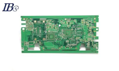
On the other hand, a PCB is a PWB that has taken the next step in the process. When electronic components such as resistors, capacitors, and integrated circuits are soldered onto the PWB, it becomes a PCB. In this state, the board can be integrated into a device and perform its function of routing electrical signals.
So, while a PWB and a PCB share a close relationship, they represent different stages in the lifecycle of an electronic board. Understanding this distinction is key to navigating the nuances of electronics.
Making a PWB is a fascinating journey involving a series of precise steps. Let’s delve into each stage to understand how a PWB comes to life.

Step 1: Designing the Circuit
The creation of a PWB begins in the virtual realm. Engineers use specialized software to design the circuit that will be printed onto the board. This design outlines the paths that electrical currents will follow to enable the device’s functionality.
Step 2: Transferring the Design
Once the circuit design is ready, it is transferred onto a copper clad PCB. This process is typically carried out using a chemical etching method, where a resist is applied to the board in the circuit design pattern. This resistance protects the copper underneath it from the upcoming etching process.
Step 3: Etching the Board
The board is then submerged in an etching solution. This solution eats away at the exposed copper, leaving only the resist-protected copper. The result is a copper pattern that matches the initial circuit design.
Step 4: Applying a Protective Coating
A protective coating is applied to protect the newly formed copper circuits from environmental damage and corrosion. This coating, often made of solder masks, also helps to prevent accidental contact between the circuits and other conductive materials.
Step 5: Drilling Holes
The final step in creating a PWB involves drilling holes for the electronic components leads. These holes, or vias, allow electrical connections through the board, linking different circuit layers.
Creating a PWB is a testament to the precision and sophistication of electronics manufacturing. Each process step is carefully controlled to ensure the resulting board can reliably route electrical signals in the intended device.

PWB assembly is a meticulous process that transforms a PWB into a fully functional PCB. Let’s break down this process into several stages to understand it better.
Step 1: Component Placement
The first step in PWB assembly involves placing the electronic components onto the PWB according to the circuit design. This step requires precision to ensure each component aligns with the corresponding conductive pathway.
Step 2: Soldering
Once the components are correctly positioned, they are soldered onto the PWB. Soldering secures the components in place and establishes electrical connections between them and the conductive pathways on the PWB.
Step 3: Inspection
After soldering, the board undergoes a thorough inspection. This step is critical to ensure the quality and functionality of the assembled board. It involves checking for potential errors, such as misplaced components or poor soldering.
Step 4: Testing
The final step in PWB assembly is testing. During this stage, the assembled board is subjected to electrical tests to ensure it functions as intended. Any issues detected during testing are addressed before the board is approved for use in an electronic device.
By understanding the process of PWB assembly, we can appreciate the precision and attention to detail required in producing electronic devices. This process ensures that each component works in harmony with others, creating functional and reliable electronic products.
Finding a reliable PWB manufacturer is crucial to ensure the success of your electronic project. Several factors can help guide your decision, ensuring you partner with a manufacturer capable of meeting your needs.

Experience and Expertise
Firstly, consider the manufacturer’s experience and expertise. A long-standing history in the industry often signifies a proven track record. Look for manufacturers who have worked on projects similar to yours, as this experience can help avoid potential pitfalls.
Quality Assurance
The quality of a PWB is paramount. Ensure the manufacturer follows strict quality control measures and meets recognized industry standards. Certifications such as ISO 9001 can be a good indicator of a manufacturer’s commitment to quality.
Turnaround Time
Consider the manufacturer’s turnaround time. How long will it take them to complete your order? Fast turnaround times can be critical, especially when working under a tight deadline.
Customer Reviews and References
Customer reviews and references can provide valuable insight into a manufacturer’s reliability and customer service. Look for manufacturers with positive reviews and satisfied customers who can vouch for their work.
Pricing
While cost should not be the sole deciding factor, ensuring that the pricing aligns with your budget is important. Compare pricing from different manufacturers, but remember that lower costs may sometimes compromise quality.
Communication
Lastly, consider how the manufacturer communicates. Do they respond promptly to your inquiries? Are they clear and transparent about their processes and pricing? Good communication is key to a successful partnership.
Latest Products

Medical Incubator PCB Board
 For PCBA
Medical Electro Cardio Graphy ECG EKG Machine PCB Assembly Board
 For PCB
Medical Blood Glucose Monitor Multilayer Printed Circuit Board Manufacturer One-stop PCB Assembly Service
 For PCB
Bar Ice Bucket Base LED Aluminum Substrate
Video Gallery