HA17358/A Series
HA17358/A Series
HA17358/A Series
- TAGS
- voltage
- hitachi
- input
- output
- frequency
- bias
- characteristics
- semiconductor
- offset
- mounting

You also want an ePaper? Increase the reach of your titles
YUMPU automatically turns print PDFs into web optimized ePapers that Google loves.
Description<br />
<strong>HA17358</strong>/A <strong>Series</strong><br />
Dual Operational Amplifier<br />
ADE-204-033 (Z)<br />
1st Edition<br />
July 2000<br />
<strong>HA17358</strong> series and <strong>HA17358</strong>A series are dual operational amplifier that provide high gain and internal<br />
phase compensation, with single power supply. They can be widely applied to control equipments and to<br />
general use.<br />
Features<br />
• Wide range of supply voltage, and single power supply used<br />
• Wide range of common mode voltage, and possible to operate with an input about 0 V, and output<br />
around 0 V is available<br />
• Frequency characteristics and input bias current are temperature compensated<br />
Features only for “A” series<br />
• Low electro-magnetic susceptibility level<br />
Vcc = +7.5 V<br />
Vee = −7.5 V<br />
Measurement Condition<br />
Rs<br />
Rs<br />
Rf<br />
0.01 μ<br />
Vin<br />
−10 dBm<br />
RF signal source<br />
(for quasi-RF noise)<br />
Rf<br />
−<br />
+<br />
V_<br />
Vout<br />
(= 100∗Vio)<br />
Output offset voltage (arb. unit)<br />
5.0<br />
4.0<br />
3.0<br />
2.0<br />
1.0<br />
0<br />
Output Offset Voltage vs. Input Interference<br />
<strong>HA17358</strong> series<br />
Improvement<br />
<strong>HA17358</strong>A series<br />
−1.0<br />
100E+3 1E+6 10E+6 100E+6 1E+9 10E+9<br />
Input RF frequency (Hz)<br />
Notice: The example of an applied circuit or combination with other equipment shown herein indicates<br />
characteristics and performance of semiconductor -applied products.<br />
The company shall assume no responsibility for any problem involving a patent caused when<br />
applying the descriptions in the example.
<strong>HA17358</strong>/A <strong>Series</strong><br />
Ordering Information<br />
<strong>HA17358</strong> <strong>Series</strong><br />
Type No. Application Package<br />
<strong>HA17358</strong> Commercial use DP-8<br />
<strong>HA17358</strong>F FP-8D<br />
<strong>HA17358</strong>A <strong>Series</strong><br />
Type No. Application Package<br />
<strong>HA17358</strong>APS Industrial use DP-8<br />
<strong>HA17358</strong>ARP FP-8DC<br />
<strong>HA17358</strong>AFP FP-8D<br />
2
Pin Arrangement<br />
Circuit Schematic (1/2)<br />
Vin(−)<br />
Vin(+)<br />
Vout1<br />
Vin(−)1<br />
Vin(+)1<br />
GND<br />
1<br />
2<br />
3<br />
4<br />
Q2 Q3<br />
Q1 Q4<br />
Q8 Q9<br />
1<br />
− +<br />
2<br />
+ −<br />
(Top View)<br />
C<br />
Q10<br />
Q11<br />
8<br />
7<br />
6<br />
5<br />
Q12<br />
V CC<br />
Vout2<br />
Vin(−)2<br />
Vin(+)2<br />
Q7<br />
Q5<br />
Q6<br />
Q13<br />
<strong>HA17358</strong>/A <strong>Series</strong><br />
R1<br />
Vout<br />
3
<strong>HA17358</strong>/A <strong>Series</strong><br />
Absolute Maximum Ratings (Ta = 25°C)<br />
Item Symbol<br />
Ratings<br />
<strong>HA17358</strong>/APS <strong>HA17358</strong>F/AFP/ARP Unit<br />
Supply voltage VCC 32 32 V<br />
Sink current Isink 50 50 mA<br />
Power dissipation PT 570 * 1<br />
385 * 2<br />
mW<br />
Common mode input voltage VCM –0.3 to VCC −0.3 to VCC V<br />
Differential input voltage Vin (diff) ±V CC ±V CC V<br />
Operating temperature Topr −20 to +75 −20 to +75 °C<br />
Storage temperature Tstg −55 to +125 −55 to +125 °C<br />
Notes: 1. This is the allowable values up to Ta = 50°C. Derate by 8.3 mW/°C.<br />
2. This is the allowable value up to Ta = 45°C mounting on 30% wiring density glass epoxy board.<br />
Derate by 7.14 mW/°C above that temperature.<br />
4
Electrical Characteristics (V CC = +15 V, Ta = 25°C)<br />
<strong>HA17358</strong>/A <strong>Series</strong><br />
Item Symbol Min Typ Max Unit Test Conditions<br />
Input offset voltage VIO — 3 7 mV VCM = 7.5V, RS = 50Ω, Rf = 50kΩ<br />
Input offset current I IO — 5 50 nA V CM = 7.5V, I IO = | I I (+) – I I (–) |<br />
Input bias current I IB — 30 250 nA V CM = 7.5V<br />
Power source rejection<br />
ratio<br />
PSRR — 93 — dB R S = 1kΩ, Rf = 100kΩ<br />
Voltage gain A VD 75 90 — dB R L = ∞, R S = 1kΩ, Rf = 100kΩ<br />
Common mode rejection<br />
ratio<br />
Common mode input<br />
voltage range<br />
Peak-to-peak output<br />
voltage<br />
CMR — 80 — dB R S = 50Ω, Rf = 5kΩ<br />
V CM (+) 13.5 — — V R S = 1kΩ, Rf = 100kΩ<br />
V CM (–) — — –0.3 V R S = 1kΩ, Rf = 100kΩ<br />
Vop-p — 13.6 — V f = 100Hz, R L = 20kΩ, R S = 1kΩ,<br />
Rf = 100kΩ<br />
+ –<br />
Output source current Iosource 20 40 — mA VIN = 1V, VIN = 0V, VOH = 10V<br />
– +<br />
Output sink current Iosink 10 20 — mA VIN = 1V, VIN = 0V, VOL = 2.5V<br />
– +<br />
Output sink current Iosink 15 50 — μA VIN = 1V, VIN = 0V,<br />
Vout = 200mV<br />
Supply current I CC — 0.8 2 mA V IN = GND, R L = ∞<br />
Slew rate SR — 0.2 — V/μs R L = ∞, V CM = 7.5V, f = 1.5kHz<br />
Channel separation CS — 120 — dB f = 1kHz<br />
5
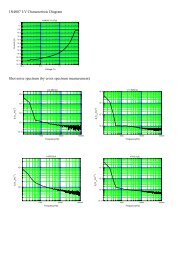
<strong>HA17358</strong>/A <strong>Series</strong><br />
Characteristic Curves<br />
6<br />
Output source current Iosource (mA)<br />
Voltage gain A VD (dB)<br />
Output Source Current vs. Ambient Temperature<br />
80<br />
70<br />
60<br />
50<br />
40<br />
30<br />
20<br />
10<br />
0<br />
VCC = 15 V<br />
VOH = 10 V<br />
−20 0 20 40 60 80<br />
Ambeint temperature Ta (°C)<br />
Supply current I CC (mA)<br />
4<br />
3<br />
2<br />
1<br />
160<br />
120<br />
Supply Current vs. Supply Voltage<br />
Ta = 25°C<br />
0 8 16 24 32 40<br />
Supply voltage VCC (V)<br />
80<br />
40<br />
Voltage Gain vs. Supply Voltage<br />
Ta = 25°C<br />
R L = ∞<br />
0 8 16 24 32 40<br />
Supply voltage VCC (V)<br />
Input bias current I IB (nA)<br />
Input bias current I IB (nA)<br />
Maximum output voltage V OP-P (V)<br />
Input Bias Current vs. Ambient Temperature<br />
80<br />
70<br />
60<br />
50<br />
40<br />
30<br />
20<br />
10<br />
0<br />
VCC = 15 V<br />
VCM = 7.5 V<br />
−20 0 20 40 60 80<br />
Ambeint temperature Ta (°C)<br />
80<br />
60<br />
40<br />
20<br />
Input Bias Current vs. Supply Voltage<br />
Ta = 25°C<br />
0 8 16 24 32 40<br />
Supply voltage VCC (V)<br />
20<br />
16<br />
12<br />
8<br />
4<br />
Maxlmum Output Voltage vs. Frequency<br />
V CC = 15 V<br />
Ta = 25°C<br />
R L = 20 kΩ<br />
0<br />
1 k 3 k 10 k 30 k 100 k 300 k<br />
Frequency f (Hz)<br />
1 M
Voltage gain A VD (dB)<br />
120<br />
100<br />
80<br />
60<br />
40<br />
20<br />
Voltage Gain vs. Frequency<br />
<strong>HA17358</strong>/A <strong>Series</strong><br />
V CC = 15V<br />
Ta = 25°C<br />
R L = ∞<br />
0<br />
1 3 10 30 100 300 1 k 3 k 10 k 30 k 100 k 300 k 1 M<br />
Frequency f (Hz)<br />
Common mode rejection ratio CMR (dB)<br />
120<br />
100<br />
80<br />
60<br />
40<br />
20<br />
Common Mode Rejection Ratio vs. Frequency<br />
V CC = 15V<br />
Ta = 25°C<br />
R S = 50 Ω<br />
0<br />
100 300 1 k 3 k 10 k 30 k 100 k 300 k 1M<br />
Frequency f (Hz)<br />
7
<strong>HA17358</strong>/A <strong>Series</strong><br />
Solder Mounting Method<br />
1. Small and light surface-mount packages require spicial attentions on solder mounting.<br />
On solder mounting, pre-heating before soldering is needed.<br />
The following figure show an example of infrared rays refow.<br />
2. The difference of thermal expansion coefficeient between mounted substrates and IC leads may cause a<br />
failure like solder peeling or soler wet, and electrical characteristics may change by thermal stress.<br />
Therefore, mounting should be done after sufficient confirmation for especially in case of ceramic<br />
substrates.<br />
8<br />
Temperature<br />
140 to 160°C<br />
235°C Max<br />
≅ 60 s<br />
1 to 5°C/s<br />
10 s Max<br />
1 to 4°C/s<br />
Time (s)<br />
Figure 1 An Example of Infrared Rays Reflow Conditions
Package Dimensions<br />
9.6<br />
10.6 Max<br />
8 5<br />
1 4<br />
0.89 1.3<br />
6.3<br />
7.4 Max<br />
0.1 Min<br />
2.54 Min 5.06 Max<br />
2.54 ± 0.25 0.48 ± 0.10<br />
1.27<br />
1.27 Max<br />
4.85<br />
5.25 Max<br />
8 5<br />
1 4<br />
*0.42 ± 0.08<br />
0.40 ± 0.06<br />
*Dimension including the plating thickness<br />
Base material dimension<br />
4.4<br />
0.75 Max<br />
0.10 ± 0.10<br />
2.03 Max<br />
0.15<br />
0.12<br />
M<br />
*0.22 ± 0.05<br />
0.20 ± 0.04<br />
0° – 15°<br />
7.62<br />
Hitachi Code<br />
JEDEC<br />
EIAJ<br />
Mass (reference value)<br />
+ 0.25<br />
6.50 – 0.15<br />
1.05<br />
+ 0.25<br />
0.60 – 0.18<br />
Hitachi Code<br />
JEDEC<br />
EIAJ<br />
Mass (reference value)<br />
+ 0.10<br />
0.25 – 0.05<br />
0° – 8°<br />
<strong>HA17358</strong>/A <strong>Series</strong><br />
DP-8<br />
Conforms<br />
Conforms<br />
0.54 g<br />
FP-8D<br />
—<br />
Conforms<br />
0.10 g<br />
Unit: mm<br />
Unit: mm<br />
9
<strong>HA17358</strong>/A <strong>Series</strong><br />
10<br />
0.75 Max<br />
1.27<br />
4.90<br />
5.3 Max<br />
8 5<br />
1 4<br />
*0.42 ± 0.08<br />
0.40 ± 0.06<br />
*Dimension including the plating thickness<br />
Base material dimension<br />
3.95<br />
+ 0.11<br />
– 0.04<br />
0.14<br />
1.75 Max<br />
0.15<br />
0.25<br />
M<br />
*0.22 ± 0.03<br />
0.20 ± 0.03<br />
6.10 + 0.10<br />
– 0.30<br />
1.08<br />
+ 0.67<br />
0.60 – 0.20<br />
Hitachi Code<br />
JEDEC<br />
EIAJ<br />
Mass (reference value)<br />
0° – 8°<br />
FP-8DC<br />
Conforms<br />
—<br />
0.085 g<br />
Unit: mm
Cautions<br />
<strong>HA17358</strong>/A <strong>Series</strong><br />
1. Hitachi neither warrants nor grants licenses of any rights of Hitachi’s or any third party’s patent,<br />
copyright, trademark, or other intellectual property rights for information contained in this document.<br />
Hitachi bears no responsibility for problems that may arise with third party’s rights, including<br />
intellectual property rights, in connection with use of the information contained in this document.<br />
2. Products and product specifications may be subject to change without notice. Confirm that you have<br />
received the latest product standards or specifications before final design, purchase or use.<br />
3. Hitachi makes every attempt to ensure that its products are of high quality and reliability. However,<br />
contact Hitachi’s sales office before using the product in an application that demands especially high<br />
quality and reliability or where its failure or malfunction may directly threaten human life or cause risk<br />
of bodily injury, such as aerospace, aeronautics, nuclear power, combustion control, transportation,<br />
traffic, safety equipment or medical equipment for life support.<br />
4. Design your application so that the product is used within the ranges guaranteed by Hitachi particularly<br />
for maximum rating, operating supply voltage range, heat radiation characteristics, installation<br />
conditions and other characteristics. Hitachi bears no responsibility for failure or damage when used<br />
beyond the guaranteed ranges. Even within the guaranteed ranges, consider normally foreseeable<br />
failure rates or failure modes in semiconductor devices and employ systemic measures such as failsafes,<br />
so that the equipment incorporating Hitachi product does not cause bodily injury, fire or other<br />
consequential damage due to operation of the Hitachi product.<br />
5. This product is not designed to be radiation resistant.<br />
6. No one is permitted to reproduce or duplicate, in any form, the whole or part of this document without<br />
written approval from Hitachi.<br />
7. Contact Hitachi’s sales office for any questions regarding this document or Hitachi semiconductor<br />
products.<br />
Hitachi, Ltd.<br />
Semiconductor & Integrated Circuits.<br />
Nippon Bldg., 2-6-2, Ohte-machi, Chiyoda-ku, Tokyo 100-0004, Japan<br />
Tel: Tokyo (03) 3270-2111 Fax: (03) 3270-5109<br />
URL NorthAmerica : http://semiconductor.hitachi.com/<br />
Europe : http://www.hitachi-eu.com/hel/ecg<br />
Asia : http://www.hitachi.com.sg/grp3/sicd<br />
Japan : http://www.hitachi.co.jp/Sicd/indx.htm<br />
For further information write to:<br />
Hitachi Semiconductor<br />
(America) Inc.<br />
179 East Tasman Drive,<br />
San Jose,CA 95134<br />
Tel: (408) 433-1990<br />
Fax: (408) 433-0223<br />
Hitachi Europe GmbH<br />
Electronic Components Group<br />
Dornacher Stra§e 3<br />
D-85622 Feldkirchen, Munich<br />
Germany<br />
Tel: (89) 9 9180-0<br />
Fax: (89) 9 29 30 00<br />
Hitachi Asia Ltd.<br />
16 Collyer Quay #20-00<br />
Hitachi Tower<br />
Singapore 049318<br />
Tel: 535-2100<br />
Fax: 535-1533<br />
Hitachi Asia (Hong Kong) Ltd.<br />
Group III (Electronic Components)<br />
7th Flr, North Tower, World Finance Centre,<br />
Harbour City, Canton Road, Tsim Sha Tsui,<br />
Kowloon, Hong Kong<br />
Tel: (2) 735 9218<br />
Fax: (2) 730 0281<br />
Hitachi Europe Ltd.<br />
Electronic Components Group.<br />
Whitebrook Park<br />
Lower Cookham Road<br />
Maidenhead<br />
Berkshire SL6 8YA, United Kingdom<br />
Tel: (1628) 585000<br />
Fax: (1628) 585160<br />
Hitachi Asia Ltd.<br />
Taipei Branch Office<br />
3rd Flr, Hung Kuo Building, No.167,<br />
Tun Hwa North Road, Taipei (105)<br />
Taiwan<br />
Tel: (2) 2718-3666<br />
Fax: (2) 2718-8180<br />
Telex: 23222 HAS-TP<br />
Telex: 40815 HITEC HX<br />
Copyright ' Hitachi, Ltd., 2000. All rights reserved. Printed in Japan.<br />
Colophon 1.0<br />
11